CircuitLeap Book a demo

One platform for
heterogeneous ICs

Multi-PDK native. Schematic, 3D layout and simulation across dies, packages and boards

4 paying customers 2 publicly traded silicon vendors Backed by Silicon Valley & European deep-tech VCs

One platform.
Every die, package and board.

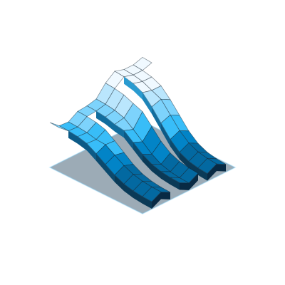
DC analysis across the IC, package, and board.

Fast GPU-native simulation in one multi-PDK workarea — benchmarked against silicon and customer tools.

Explore
Faster and more accurate than existing solutions — customer benchmarked.
Launch as many cloud simulations in parallel as you need — no seat ceiling.
Swap processes and packages without rebuilding the project.
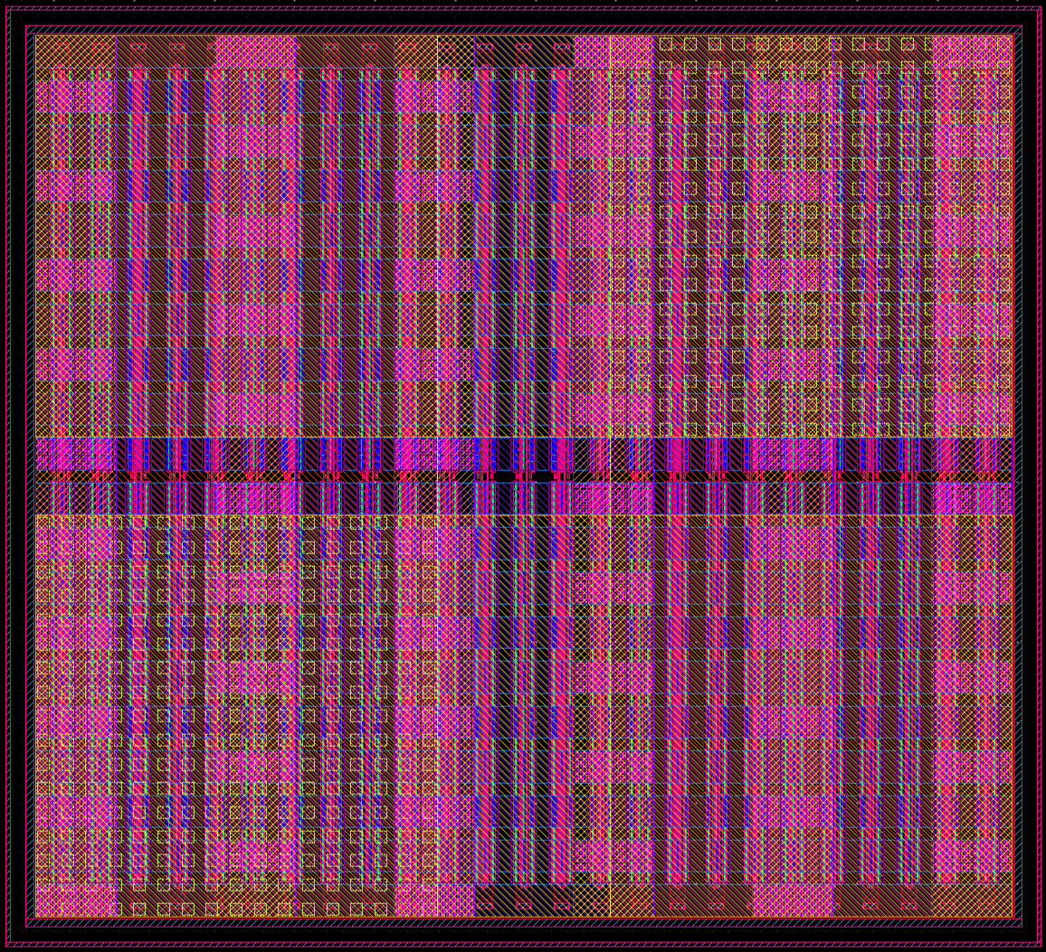
AI Design Generation

AI-based design generation for complete analog layouts.

Explore
Preserve your metallization style and apply it automatically to every new design.
Edit schematic and layout together in natural language.

Time-domain simulation

GPU-native transient RLCM: the complete system over time, not a single DC snapshot.

Explore
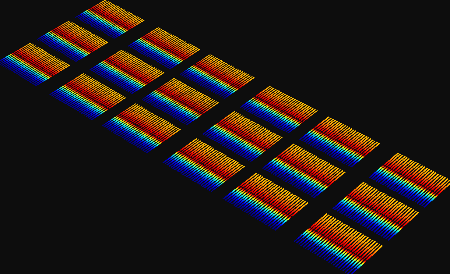
Visualize your results in 4D — X, Y, Z and time — and pick any point in your layout to plot over time.
Resistance, capacitance, self-inductance, and mutual inductance.
Heterogeneous by design

Many process nodes. One design.

Built multi-PDK native for heterogeneous ICs — dies from different processes, advanced packaging and the board, designed together.

Load several process PDKs — plus package and board — into one project, each valid in its own 3D region.
Design with components from every loaded PDK. CircuitLeap keeps each node’s schematic and layout separated behind the scenes.
Simulate across die, package and board — with simultaneous multi-PDK, multi-die analysis on the way.
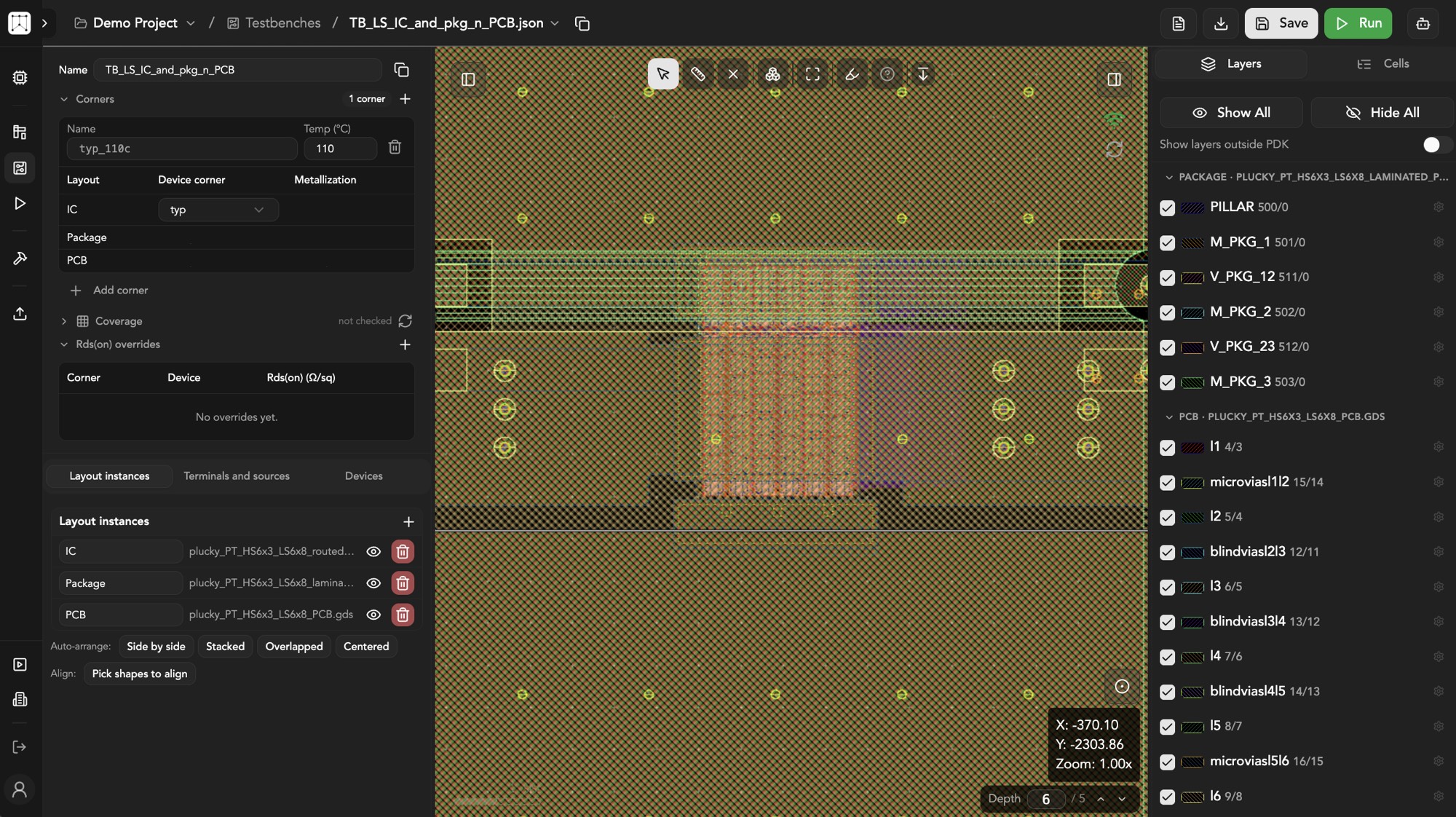
A CircuitLeap testbench holding an IC, its package and the PCB as one project, with the package and board layer stacks listed beside the layout
One testbench — the IC, its package and the board, in one project
Clai

Make AI your co-worker.

Build a PDK from the documents you have. Edit your layout in plain words. When a value is missing, Clai asks instead of assuming.

Screenshots and spreadsheet read
Layer stack extracted
Missing the RDL thickness and EM rule — use 10 µm and standard copper?
EDA integration

Your flow, connected.

A plugin links CircuitLeap to the established EDA environment your team already uses. Bring designs and PDKs in, work at full speed here, and hand validated designs back for signoff.

Your EDAdesigns in · designs backCircuitLeap

Traction

Four paying customers run CircuitLeap in commercial production — two of them large, publicly traded silicon vendors.

Backed by a blend of Silicon Valley and European deep-tech investors.


Mission

CircuitLeap is transforming analog and heterogeneous IC design by leveraging large-scale parallel computing and an AI-driven workflow.

01

Purpose

We empower organizations to optimize designs end-to-end, removing tedious manual steps and massively speeding up design cycles. Our goal: keep you ahead of the competition.

02

Approach

We unite deep domain expertise with world-class math, AI, and distributed compute. We believe in true collaboration to reinvent circuit design from the ground up.

03

Impact

We focus on customers where accelerating innovation is key to staying competitive. By enabling faster breakthroughs, we help you remain at the cutting edge.


Small team,
deep stack

Device physicists, solver engineers and product people who have shipped analog silicon and know exactly where the flow hurts.

We work close to our users. Most features start as a conversation with someone mid-tapeout.

We are hiring

David Tournatory
Co-founder & CEO
Founded Gazelle Semiconductor, acquired by Silergy. Six Silicon Valley startups from Volterra onwards, over fifteen patents, and teams led across the US, the UK and Singapore.
Nuno Lourenço
Co-founder & CTO
Over twenty years automating analog design at Instituto de Telecomunicações, and taught it at Instituto Superior Técnico. More than fifty publications, from patents and books to journals and conference papers.
Nathan Rigalle
Co-founder
Builds the numerical solvers at the platform’s core. Computational and applied mathematics at La Rochelle Université, and taught at EIGSI engineering school.

See it on your own design.

Bring your design. We will run it with you, on a call, in no time.